
A global leader in radiation detection and safety faced critical efficiency and yield challenges during the assembly and testing phase of their neutron detector sensor chips. The indispensable wafer dicing process – whether utilizing saws or lasers – created atomic-scale defects and contamination, that introduced large variation and Signal-to-noise levels for their detector sensor chips.
This defect generation led directly to 3 major issues:
- High electrical variance: Large variation in the leakage currents resulted in highly variable chip properties, necessitating time-consuming and costly manual calibration.
- Low Signal-to-noise Ratio: Due to high leakage current, the final solution was not able to detect small doses well, impacting to overall quality of the product.
- Lower manufacturing yield: The electrical instability forced the use of thicker safety margins around the chip edges, sacrificing valuable active area and reducing overall manufacturing yield.
The customer required a reliable solution to reduce this variability and enable the adoption of thinner safety margins, provided the solution’s beneficial effects with good reliability.
The SisuSemi solution: Defect reduction and sidewall passivation
SisuSemi proposed a specialized surface treatment designed to clean & passivate sidewall defects and reduce contamination immediately following the dicing process.
Key results and technical validation
The results confirmed the robustness and immediate benefit of the SisuSemi solution:
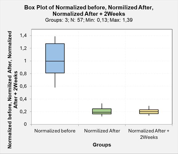
- Leakage current reduction: As average up to 80% reduction for absolute leakage current was achieved within test population. This drives a better signal-to-noise ratio, enabling customers to achieve better sensitivity for low doses.
- Variation reduction: Over 75% reduction in variation (measured as Standard Deviation, StDev) for leakage current, helping to reduce the calibration time and improve part-to-part similarity.
- Durability and Stability: The leakage current and variation reduction is visible after 2 weeks, without chip packaging, indicating good stability.
Conclusion: Driving substantial operational impact
By preserving the reduced defect density and contamination levels, the SisuSemi solution directly translates into:
- Reduced variance: Minimizing the need for costly manual calibration work.
- Boost performance: Reduced leakage current drives improved signal-to-noise ratio, enabling better sensors.
- Increased yield: Enabling the customer to employ thinner safety margins at the chip edges.
SisuSemi’s technology offers a highly reliable method to stabilize semiconductor properties immediately post-dicing, unlocking significant improvements in assembly efficiency and delivering a measurable boost to manufacturing yield.
 Share
Share
 Tweet
Tweet
 Share
Share
 Share
Share