
Connecting surface quality to device performance in semiconductor manufacturing
A semiconductor surface can meet its roughness specification while the finished device still shows excessive leakage or unstable electrical characteristics. This is important when it threatens a device specification, reduces electrical yield or delays qualification.
If established process adjustments have not resolved the problem, a surface or interface contribution may be worth investigating. The starting point is an observed device limitation and a testable hypothesis about its cause. Atomic-level defects are one possible explanation – their importance must be established for the product and process concerned.
A review published in Nanomanufacturing and Metrology in September 2026 examines plasma-based atom-selective etching (PASE), an atmospheric plasma process for selectively removing surface atoms. The authors describe progress in atomic-scale polishing, alongside challenges in uniformity, thermal stress and oxidation.
The authors note that devices based on PASE-polished surfaces had not yet been reported in the literature they reviewed. They also flag potential electronic defects from plasma-generated ultraviolet radiation. This reinforces the need to connect surface measurements to device results.
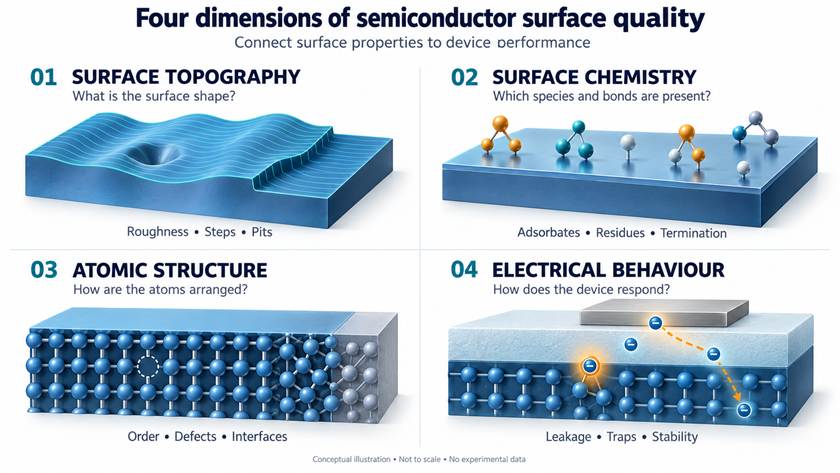
Four complementary views of semiconductor surface quality. Conceptual illustration, not to scale and not experimental data.
The illustration separates four complementary questions. Surface topography describes roughness, steps and pits. Surface chemistry concerns residues, adsorbates and the intended termination. Atomic structure concerns ordering and defects near the surface or interface. Electrical measurements show how the resulting structure or device responds under the tested conditions.
For an IDM, foundry or OSAT, the useful connection is between a change in those surface properties and the device parameter that limits the product. Evidence of a smoother surface or a more ordered interface needs to be linked to electrical performance before drawing conclusions about yield or reliability.
At SisuSemi, this connection guides how we propose evaluating Atomic-Level Purification (ALP). Our process uses ultra-high vacuum, temperatures below 450 °C and controlled oxidation. It is designed to clean silicon surfaces, improve atomic ordering and form a thin protective silicon dioxide layer. Suitability depends on the material stack, temperature exposure and requirements of the following process steps.
Our company-reported metal–oxide–semiconductor capacitor (MOSCap) case summary describes an evaluation involving a silicon/aluminium oxide interface. ALP-treated structures showed a 42% reduction in interface defect density and a 67% reduction in leakage current compared with a chemically grown oxide reference. The summary also reports structural characterization by scanning transmission electron microscopy. These results concern the tested structures and conditions – another device or manufacturing route needs its own comparison.
The case summary does not provide absolute electrical values, detailed measurement conditions, sample counts or distributions. Those details need to be reviewed before judging transferability. A technical comparison should also establish the dielectric stack, thickness, thermal history and other differences between treated and reference samples. This helps assess whether the results support the proposed mechanism and whether the comparison represents the customer’s process.
A useful feasibility study starts with the affected product requirement and the minimum improvement that would matter. The team should define the electrical metric, reference process and stopping criteria, including unacceptable changes in other critical parameters. Matched reference and treated samples should receive equivalent subsequent processing and measurement conditions. Where practical, the comparison should include the customer’s best feasible alternative treatment.
Surface analysis then helps interpret the result. If the electrical response changes, which chemical or structural changes could explain it? If it does not, what does that reveal about the original hypothesis? Results should be assessed against measurement uncertainty and sample variability. Further development should test whether the benefit is reproducible, improves the relevant device distribution and survives subsequent fabrication, packaging and appropriate stress testing.
Before requesting samples, the teams should identify a candidate insertion point and screen the material stack, full temperature exposure, oxidation requirements and handling route. An off-line evaluation may be suitable if representative downstream testing can be arranged. The process and device owners should agree how treated material would proceed through that route and what would make the evaluation stop. Repeatability, total cycle time and cost per good device then inform the case for further development.
A technical gain should have a credible route to business value, such as more devices meeting specification, less scrap or a qualification issue resolved. That value must justify evaluation, integration and operating costs. Continuing with the current process or making a simpler adjustment remains a valid outcome when it meets the product’s needs.
If an unresolved electrical issue is affecting your product performance or manufacturing results, contact SisuSemi for an initial applicability discussion. You can start with an anonymized description of the symptom, the metric that matters and broad process constraints. Together, we can assess whether a surface or interface contribution is plausible and whether an ALP comparison is worth designing. A feasibility study would follow if the problem, compatibility and value of the proposed test justify it.
 Share
 Tweet
 Share
 Share