
As the semiconductor industry advances toward smaller node sizes and increasingly complex 2D structures, precise pattern control has become more critical than ever. This trend has long driven the development of high-performance dry-etching technologies that enable accurate patterning at the nanoscale.
However, despite their advantages, dry-etching methods also introduce several critical challenges that continue to impact device performance.
Dry-Etching Defects – Hidden Challenges at the Atomic Scale
Chemical residuals are one of the defects caused by dry-etching, as highlighted by K. Yang et al. in their article [1]. In addition to surface contamination, dry-etching processes can cause atomic-level and sub-surface defects that are detrimental to final device performance.
Emerging techniques such as Atomic Layer Deposition (ALD), Atomic Layer Etching (ALE), and Neutral Beam Etching (NBE), discussed by T.Y. Lee et al. [2], have helped mitigate some of these issues and have become foundational for next-generation device fabrication.
Still, even these advanced methods can introduce atomic-level imperfections that must be addressed.
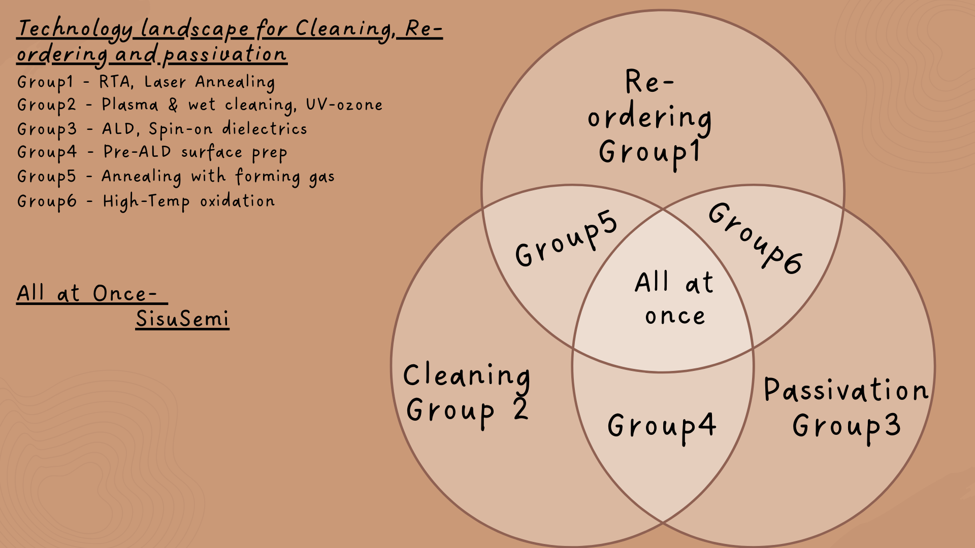
The Three Critical Issues – Cleaning, Re-ordering, and Passivation
To achieve optimal device performance, three interdependent challenges must be solved:
Cleaning / Contaminant Removal
Extensive research has focused on reducing dry-etching residuals and eliminating natural contaminants like carbon and hydrogen. However, fully removing these impurities remains a challenge. Even minimal contamination on the semiconductor surface can degrade device yield and reliability in downstream processes.Re-ordering of Atomic Structure
For next-generation 2D materials and devices with extremely small node sizes, traditional thermal techniques such as Rapid Thermal Annealing (RTA) are not viable due to the thermal fragility of these structures. Re-ordering the atomic lattice without damaging these materials requires a new approach.Passivation
Technologies like ALD have significantly improved passivation quality over legacy techniques. However, when working with ultrathin layers, sometimes just a few monolayers, pinholes and other defects remain a concern. A high-quality passivation layer requires a contaminant-free and atomically ordered surface to begin with.
Addressing any one of these issues is a step forward, but addressing all three in unison is essential for next-generation device performance.
A Holistic Solution from SisuSemi – All in one process
At SisuSemi, we offer a novel solution that tackles all three issues simultaneously. Our technology cleans wafers from atomic-level contaminants in an ultra-high-vacuum environment at slightly elevated temperatures.
This novel process:
- Removes atomic-level contaminants
- Reorders the atomic structure without damaging delicate 2D materials
- Grows a thin, stable crystalline SiO2 layer for superior passivation
The result is a clean, smooth, and ordered surface that enables the integration of high-performance nanoscale device layers with minimal defects.
Conclusion
Achieving optimal semiconductor performance requires more than incremental improvements. Cleaning, re-ordering, and passivation must all be addressed simultaneously. At SisuSemi, we offer a comprehensive, production-ready solution designed to meet the demands of the most advanced semiconductor nodes.
Let’s redefine what’s possible in semiconductor manufacturing—together.
References
[1] https://ieeexplore.ieee.org/document/9792508
[2] https://pubs.rsc.org/en/content/articlehtml/2025/na/d4na00784k
 Share
Share
 Tweet
Tweet
 Share
Share
 Share
Share