
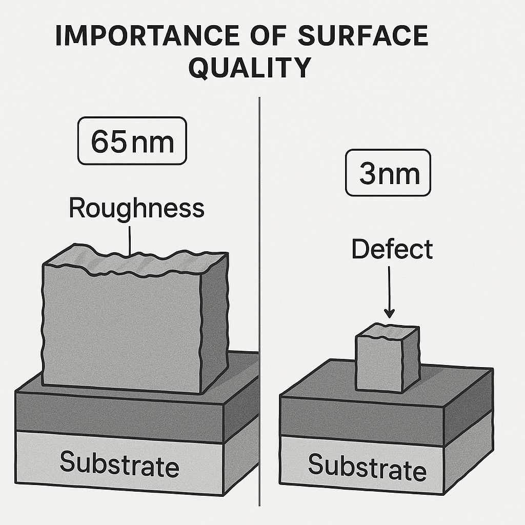
The surface quality and roughness that were still acceptable with 60nm+ linewidths become catastrophic at node sizes of 10 nm and below. With smaller nodes, transistors are mainly constructed from a surface, increasing the importance of atomic-level cleanliness and smoothness.
In semiconductor fabrication, engineers have focused on minimizing defects for decades. However, as node sizes decrease, traditional methods targeting particles and larger contaminants are no longer sufficient. To maintain performance and reliability, it is essential to improve cleanliness and surface quality at the atomic level.
Research supports this need. For example, Chen et al. (https://ieeexplore.ieee.org/document/1210828) emphasize that with CMOS technology, the quality of the Si-SiO₂ interface becomes critical when scaling below 100nm dimensions. Classical cleaning and preparation methods do not always provide the best interface quality, since the root causes lie in the atomic-level structure of silicon and silicon dioxide.
Sources of Poor Smoothness and Si-SiO₂ Quality Issues
Poor surface smoothness and interface quality typically stem from two main factors:
- Silicon Surface Quality: The silicon surface is the starting point. Contaminants such as carbon, hydrogen, and oxygen cause atomic-level roughness. Even after cleaning, non-ordered silicon atoms remain near the surface due to prior processing steps and bonds with contaminants.
- SiO₂ Quality: Native oxide is non-crystalline, and most oxidation methods do not produce crystalline surfaces. Consequently, even initially smooth surfaces can result in poor SiO₂ interface quality.
Effects of Poor Si-SiO₂ Quality
Poor interface quality impacts transistor and chip performance. Key effects reported by Chen et al. include:
- Oxide Thickness and Roughness: Reducing interface roughness improves chip characteristics.
- Drive Currents and Mobility: Devices with reduced interface roughness (~1.1 Å rms) showed improved drive currents: 5% for NMOS and 17% for PMOS transistors. Smoother interfaces enhance carrier mobility and overall electrical performance.
- Transistor Performance: Transconductance improved for both NMOS and PMOS devices, demonstrating better current-voltage characteristics and confirming that optimized interface roughness directly enhances transistor performance.
SisuSemi’s work aligns with these findings. Our advanced surface treatment technology can significantly reduce interface roughness, leading to enhanced chip characteristics. Demonstrated improvements include a 42% reduction in interface defect density (boosting carrier mobility and reducing energy losses) and a 67% reduction in leakage current (enhancing power efficiency and reliability). Optimizing the oxide interface directly improves transistor current-voltage behavior and overall device stability.
Solution
While multiple solutions exist, classical methods do not address all sources of roughness. SisuSemi’s novel solution provides state-of-the-art surface quality for semiconductor fabrication. Using vacuum technology and elevated temperatures, it:
- Removes contaminants from the surface,
- Re-orders atoms near the surface, and
- Provides a smooth, crystalline SiO₂ protective layer.
Conclusion
As node sizes shrink, surface effects become a dominant factor in transistor performance. Without atomic-level cleanliness and a smooth protective layer, active defects persist, compromising device performance and reliability. While classical solutions address some issues, SisuSemi’s advanced approach tackles all sources of poor interface quality, enabling superior semiconductor performance.
*) Image created with ChatGPT for illustrative purposes
 Share
Share
 Tweet
Tweet
 Share
Share
 Share
Share