
In the relentless pursuit of smaller, faster, and more powerful semiconductor devices, the industry faces an escalating challenge: atomic-level defects and contamination. These microscopic imperfections, often invisible, can have catastrophic consequences for device performance, reliability, and manufacturing yield. From a single misplaced atom to a nanometer-sized particle, these issues are the silent saboteurs of chip production.
Atomic-level defects can be intrinsic to the semiconductor material (vacancies, interstitial atoms, antisite defects) or extrinsic (unintentional foreign atom incorporation). Contamination encompasses any unwanted material—particles, chemical residues or airborne molecular contaminants—that compromises wafer integrity. Sources are ubiquitous: process chemicals, equipment, cleanroom environment, and human contact. The stakes are incredibly high; contamination significantly impacts yield, profitability, and time-to-market.
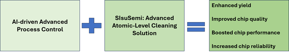
Traditionally, manufacturers relied on stringent cleanroom protocols, careful process control, and advanced inspection. However, as feature sizes shrink, the sheer volume of data overwhelms conventional methods. This is where Artificial Intelligence (AI) and Machine Learning (ML) emerge as game-changers, ushering in a new era of Advanced Process Control (APC). When combined with an advanced atomic-level cleaning solution, like the SisuSemi one, results in significantly improved chip performance and quality, as well as manufacturing yield.
The AI revolution in Advanced Process Control
AI-driven APC is a paradigm shift in quality and yield management. By leveraging big data analytics, pattern recognition, and predictive modelling, AI systems proactively identify, mitigate, and even prevent defect and contamination formation. The core principle is to move beyond reactive troubleshooting to a proactive, intelligent manufacturing environment.
Benefits of AI-Driven APC:
- Unprecedented defect detection and classification: AI algorithms, particularly deep learning, excel at analyzing vast image data from optical inspection tools. They detect and classify defects with remarkable accuracy (over 99%), including subtle or unknown types, surpassing human capabilities. This precision allows for rapid identification of problematic areas and targeted corrective actions.
- Proactive anomaly detection and predictive maintenance: AI analyzes real-time and historical manufacturing data to identify minute deviations that precede defect or contamination events. Predictive models forecast potential issues, enabling proactive equipment maintenance or process adjustments, preventing costly downtime and yield excursions.
- Enhanced yield optimization: AI-driven yield management integrates advanced analytical tools across the manufacturing flow. By continuously monitoring process parameters and correlating them with yield data, AI identifies critical factors and suggests optimal operating conditions. This data-driven approach has demonstrated significant reductions in overall yield detraction, with some reports indicating improvements of up to 30%.
- Real-time process control and optimization: AI can be integrated directly into process tools for real-time, closed-loop control. By continuously analyzing sensor data, AI makes immediate, fine-tuned adjustments to parameters like gas flows, temperatures, and pressures. This dynamic optimization minimizes process variations that lead to defects and contamination, leading to measurable improvements in process efficiency.
- Accelerated root cause analysis: When defects occur, AI significantly shortens root cause analysis time. By correlating defect patterns with historical process data, equipment logs, and material inputs, AI rapidly identifies probable causes, allowing engineers to implement effective corrective actions much faster.
The limitations of AI-APC: A Complementary Approach is Key
While AI-driven APC offers transformative benefits, it is crucial to understand its inherent limitations. AI is a software-based solution; it cannot physically remove atomic-level defects or contamination once formed. Its power lies in its ability to prevent, detect, and mitigate these issues through intelligent process management.
For example, AI can predict a tool will generate particles or detect a tiny contaminant. However, it cannot physically clean the tool or remove the particle. These actions require physical interventions: advanced cleaning processes, equipment maintenance, or specialized defect removal techniques.
This distinction highlights a critical point: AI-driven APC should not be viewed as a standalone cure-all, but rather as a powerful complement to physical defect and contamination removal solutions. The most effective strategy involves a tandem approach, where AI optimizes manufacturing to minimize defect formation, and specialized physical solutions address defects and contamination that inevitably arise.
An excellent example of such a complementary solution is SisuSemi. SisuSemi specializes in technologies that directly address atomic-level defects and contamination on semiconductor surfaces. By integrating SisuSemi’s physical defect removal capabilities with AI-driven APC, manufacturers can achieve a truly comprehensive and robust quality control ecosystem. AI ensures the process is as clean and optimized as possible, while SisuSemi provides the means to physically rectify any remaining imperfections, leading to unparalleled yield, device quality, performance, and reliability.
Conclusion: The future is hybrid
The semiconductor industry faces stringent demands for precision and purity. Atomic-level defects and contamination require a sophisticated, intelligent approach. AI-driven Advanced Process Control offers a powerful solution, revolutionizing defect detection, process optimization, and yield management.
However, AI-APC is a force multiplier, not a standalone magic bullet. While AI predicts, detects, and optimizes to minimize defects, it cannot physically remove them. The ultimate success lies in a hybrid strategy: leveraging AI’s predictive and analytical prowess in tandem with advanced physical defect and contamination removal solutions. Companies like SisuSemi, focusing on direct atomic-level remediation, represent the crucial other half of this equation.
For semiconductor professionals, the message is clear: embrace AI-APC for its unparalleled capabilities in process intelligence and optimization. But simultaneously, invest in and integrate physical solutions that can address inevitable imperfections. This dual approach—intelligent prevention coupled with precise remediation—is the true path to unlocking the next generation of high-yield, high-performance semiconductor manufacturing. The future of chipmaking is not just intelligent; it is intelligently integrated.
 Share
Share
 Tweet
Tweet
 Share
Share
 Share
Share