
Blog
Search for the insights

25/09/2026
Why Hardware Makes Deep Tech a Better Bet: The Investment Case for SisuSemi’s ALP Platform
Venture investors have spent the last decade rewarding software for its margins and speed of scale, and hardware has often been treated as the slower,
Read More →
11/09/2026
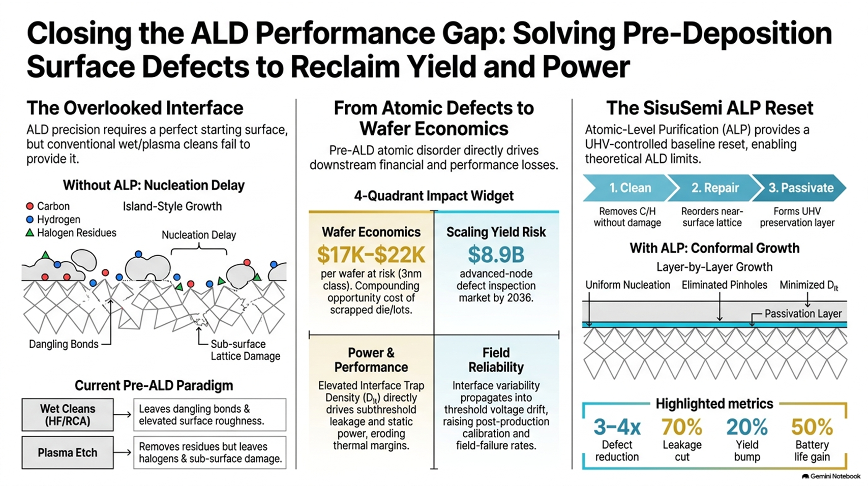
When the Foundation Cracks: How Pre-ALD Surface Defects Undermine Atomic Layer Deposition
Atomic Layer Deposition has earned its place as the workhorse of advanced-node manufacturing. Its self-limiting, layer-by-layer chemistry gives fabs something no other deposition method can
Read More →
04/09/2026
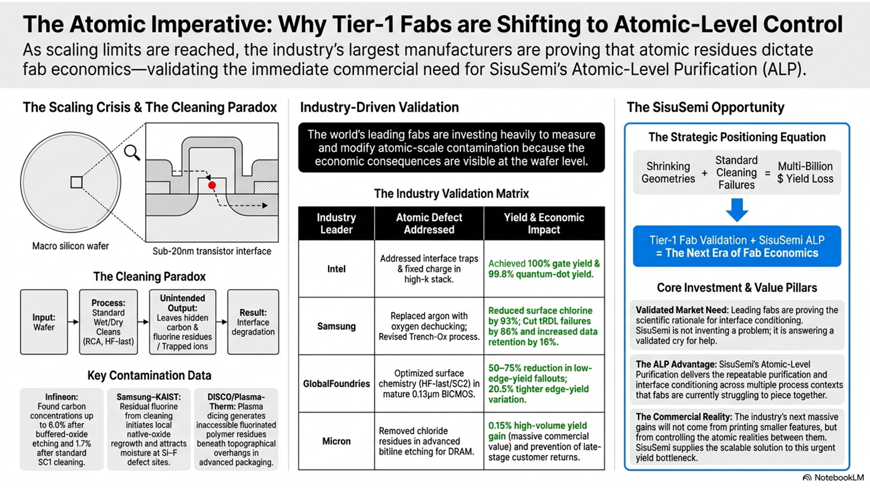
The Industry Is Looking Deeper: Why Atomic-Level Defects and Contamination Have Become a Strategic Semiconductor Priority
For decades, semiconductor manufacturing progress was described mainly through lithography, transistor dimensions and wafer-scale yield. The research papers reviewed here show that the industry’s attention
Read More →
28/08/2026
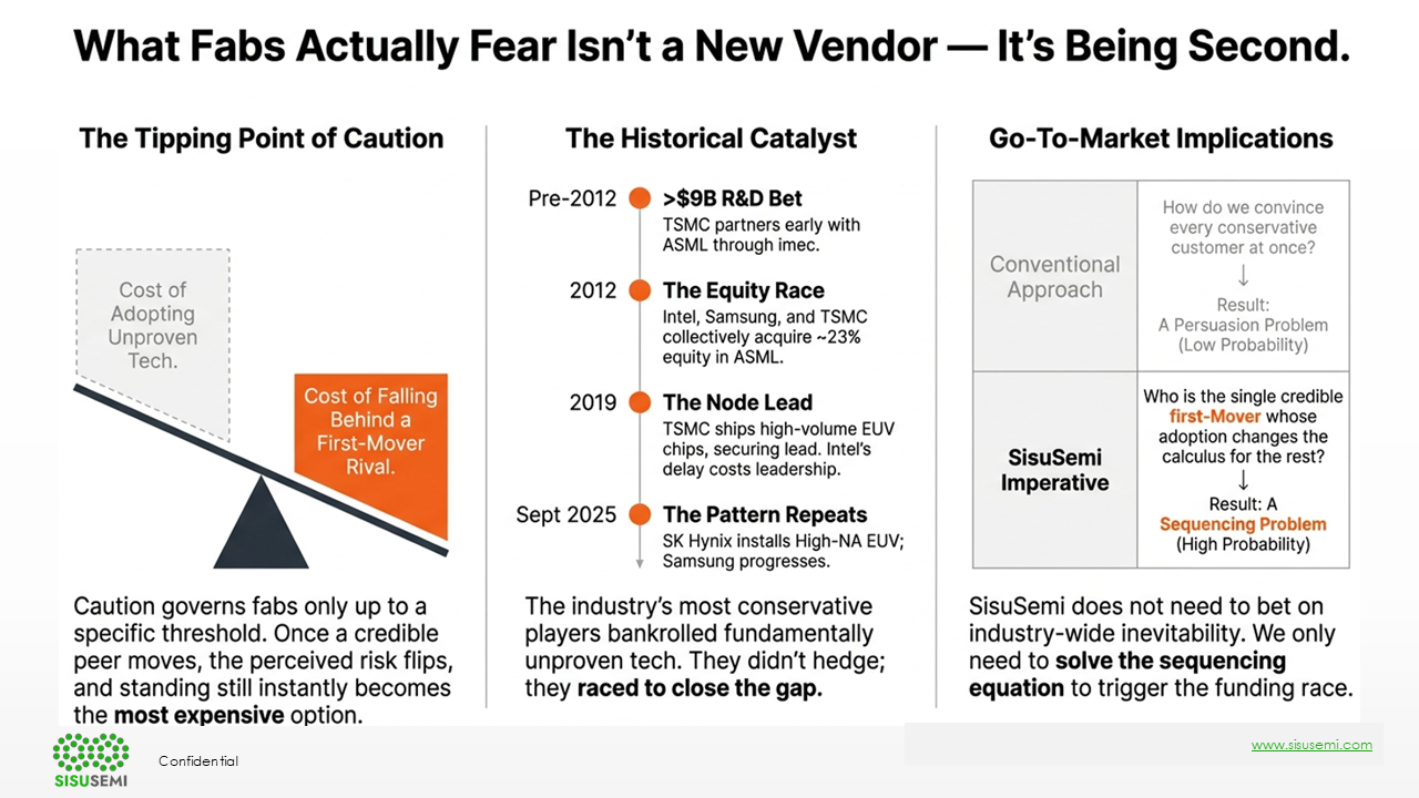
What Fabs Actually Fear Isn’t a New Vendor – It’s Being Second
The typical assumption about semiconductor manufacturers is that they’re conservative almost by temperament: risk-averse, slow to change, unwilling to bet a production line on anything
Read More →
21/08/2026
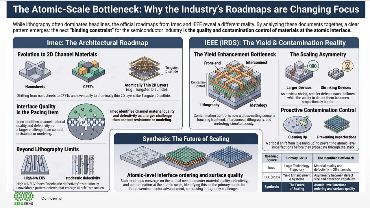
What the Public Roadmaps Signal About the Next Atomic-Scale Bottleneck
Roadmaps are the least hyped documents in the semiconductor industry, which is exactly what makes them worth reading closely. Nobody is trying to raise money
Read More →
14/08/2026
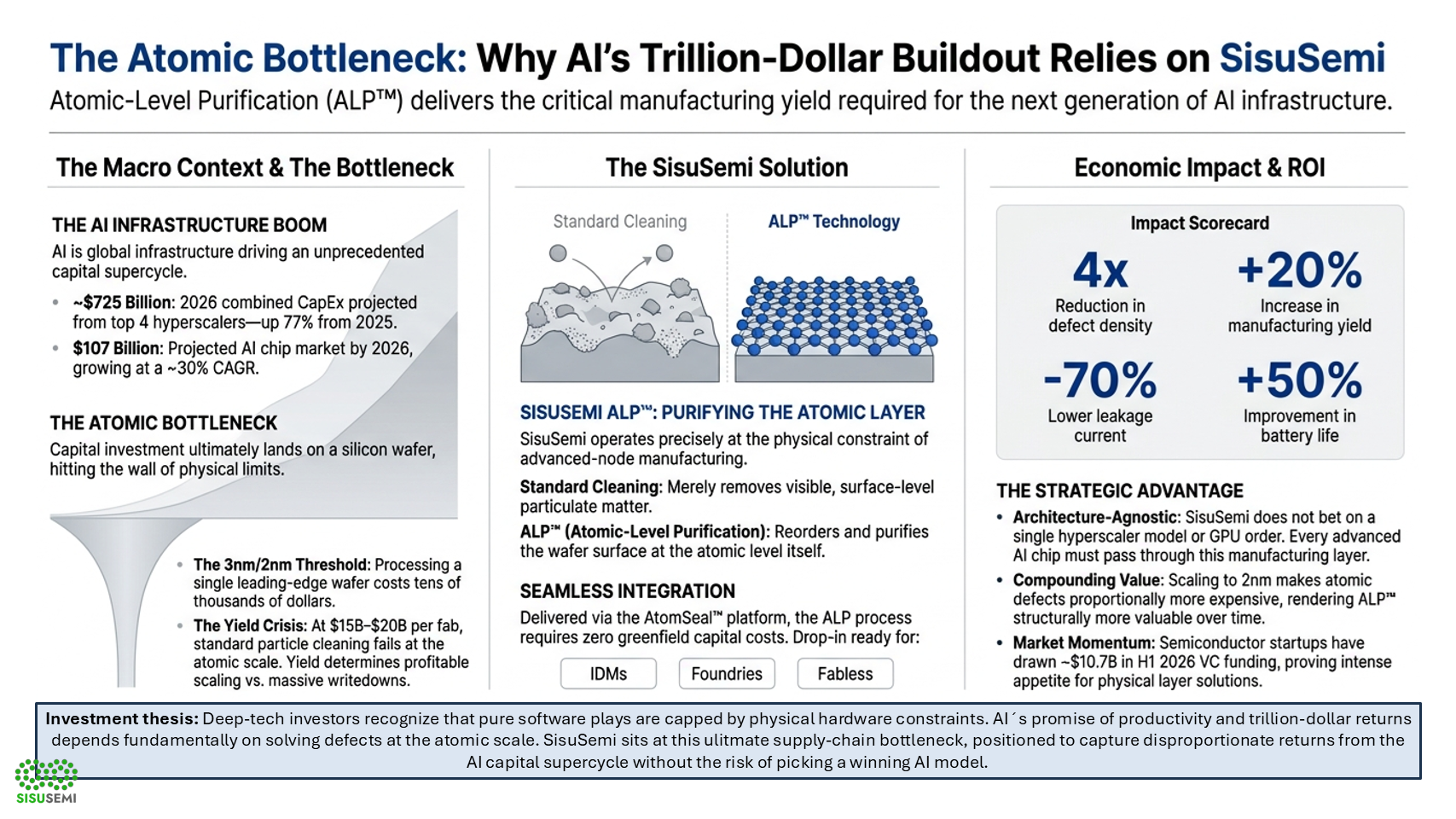
The Atomic Bottleneck: Why AI’s Trillion-Dollar Bet Runs Through Semiconductor Purity
Artificial intelligence has stopped being a demo and become infrastructure. In under three years, models like ChatGPT, Claude and Gemini have moved from research curiosities
Read More →
03/07/2026
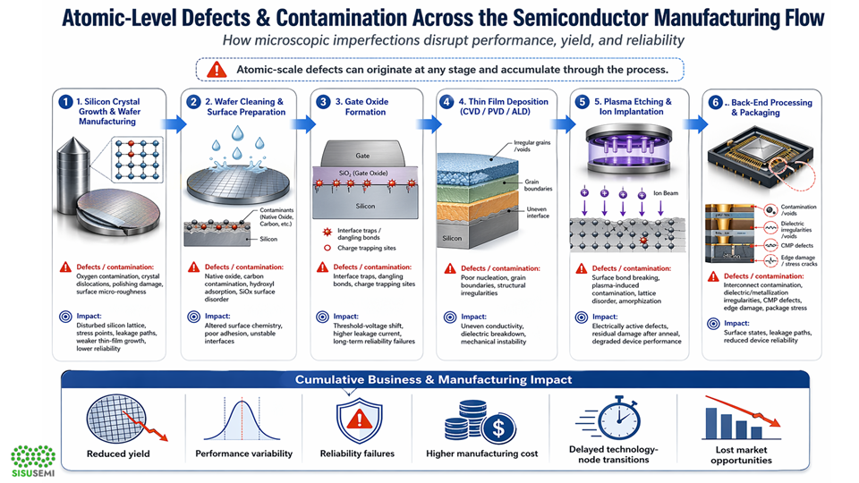
Atomic-Level Defects and Contamination in Semiconductor Manufacturing: Challenges, Business Impact and Future Opportunities
Semiconductor manufacturing is one of the most precise industrial processes ever developed. Modern chips are fabricated at nanometer scales where even a single misplaced atom
Read More →

26/06/2026
Oxide-Free Interfaces: The Problem No One Sees But Everyone Pays For
Modern semiconductor manufacturing assumes that a clean silicon surface is “good enough” after standard HF-last processing. In reality, this is not the case. After the
Read More →
05/06/2026
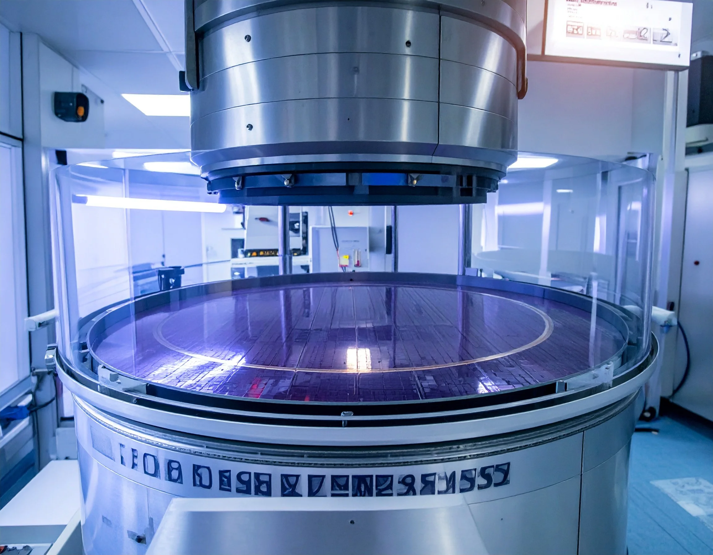
Bridging the Gap: Overcoming Atomic-Level Challenges in Heterogeneous Integration
In the pursuit of More-than-Moore scaling, wafer bonding has emerged as a cornerstone of heterogeneous integration. By enabling the fusion of disparate materials—such as GaN-on-Silicon
Read More →

22/05/2026
When Every Atom Counts: How Atomic-Level Defects Are Redefining MOSCap Performance — and the Business Case for Solving Them
For decades, the semiconductor industry managed defects the way you manage visible dirt: with progressively finer filters, cleaner rooms and tighter process controls aimed at
Read More →