
Semiconductor manufacturing is one of the most precise industrial processes ever developed. Modern chips are fabricated at nanometer scales where even a single misplaced atom can influence device behavior. As a result, atomic-level defects and contamination have become critical challenges across the semiconductor manufacturing process flow, affecting device performance, reliability and production economics. Understanding where these defects originate and how they impact manufacturing outcomes is essential for chipmakers striving to maintain competitiveness in an increasingly demanding industry.
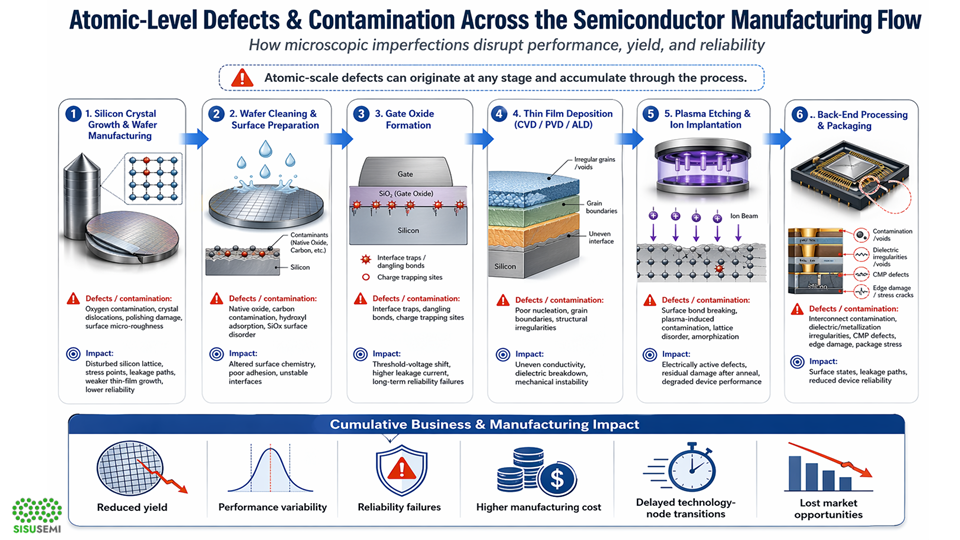
The semiconductor manufacturing process consists of multiple stages, from silicon crystal growth to advanced packaging and electrical testing. At each stage, atomic-scale imperfections can appear due to material interactions, process conditions or contamination. These defects may accumulate throughout the process flow and ultimately affect the functionality of the final device.
Defects during silicon crystal growth and wafer manufacturing
The manufacturing process begins with silicon crystal growth, where highly pure single-crystal silicon ingots are produced. At this stage, contamination by oxygen or the formation of crystal dislocations can occur. Such defects disturb the regular atomic arrangement of the silicon lattice and may later act as recombination centers or leakage paths in semiconductor devices.
During wafer manufacturing, processes such as slicing, lapping, and chemical mechanical polishing (CMP) shape the silicon ingot into flat wafers. These mechanical and chemical treatments introduce risks such as polishing damage and surface micro-roughness. Even small disruptions in the atomic structure of the wafer surface can create localized stress points that later affect thin film growth and device reliability.
Contamination during wafer cleaning and surface preparation
Once the wafer is prepared, it undergoes RCA cleaning to remove particles and organic contaminants. However, even cleaning processes can introduce atomic-scale challenges. Issues such as native oxide formation, carbon contamination and hydroxyl group adsorption can alter the chemical state of the silicon surface.
These contaminants can produce an amorphous silicon oxide (SiOx) layer or surface disorder, which interferes with subsequent processing steps. When later layers are deposited, the presence of these surface defects can degrade adhesion and cause interface instability.
Interface defects in gate oxide formation
One of the most critical stages in semiconductor manufacturing is gate oxide formation. The interface between silicon and its oxide layer determines how effectively a transistor controls electrical current. At the atomic level, defects such as interface traps, dangling bonds and charge trapping sites can emerge.
These imperfections alter the electrical characteristics of transistors, leading to problems such as threshold voltage shifts, increased leakage current and long-term reliability failures. In advanced device architectures such as FinFETs or gate-all-around (GAA) transistors, the sensitivity to interface defects becomes even greater because the devices operate at extremely small dimensions.
Thin film deposition and structural imperfections
Thin films are deposited during many steps of chip fabrication using techniques such as chemical vapor deposition (CVD), physical vapor deposition (PVD) and atomic layer deposition (ALD). At the atomic scale, poor nucleation or the formation of grain boundaries can introduce structural irregularities in deposited materials.
These imperfections may lead to uneven electrical conductivity, dielectric breakdown or mechanical instability. In multilayer device structures, even minor film defects can propagate and impact subsequent process steps, compounding reliability issues.
Plasma etching and ion implantation damage
After lithography defines circuit patterns, plasma etching removes material to create device features. However, energetic plasma environments can cause surface bond breaking, dangling bonds and plasma-induced contamination. These atomic disruptions alter surface chemistry and may introduce electrically active defects.
Similarly, ion implantation, which introduces dopant atoms into the silicon lattice, can cause lattice disorder and amorphization. Although subsequent annealing processes are designed to repair the crystal structure, incomplete recovery can leave residual defects that degrade device performance.
Defects during back-end processing and packaging
Atomic-scale damage is not limited to front-end transistor fabrication. During interconnect formation, dielectric deposition, metallization and CMP processes can introduce surface irregularities or contamination.
Later steps such as wafer backgrinding and dicing may damage silicon bonds at the wafer edges, creating surface states and leakage paths that affect device reliability. Even packaging processes can introduce stress that interacts with underlying atomic defects.
Business impact of atomic-level defects
Atomic-scale defects have significant business consequences for semiconductor manufacturers. The most direct impact is reduced yield, where a percentage of chips on a wafer fail electrical testing due to defects. Because semiconductor fabrication facilities cost billions of dollars to operate, even small yield losses translate into substantial financial impact.
Defects also affect product reliability and field performance, potentially leading to warranty claims, product recalls, or reputational damage. Furthermore, as device geometries shrink below 5 nm, the margin for error becomes extremely small, increasing the risk that atomic-scale contamination could delay technology node transitions.
In competitive markets such as AI processors, automotive electronics and advanced memory, manufacturing defects can also lead to lost market opportunities, slower product launches and reduced profitability.
Opportunities if atomic-level defects are controlled
Despite these challenges, the ability to control atomic-level defects presents significant opportunities for semiconductor manufacturers.
First, improved defect control directly enhances manufacturing yield and cost efficiency. Even a small percentage increase in yield can generate millions of dollars in additional revenue per production line.
Second, better contamination control enables the development of smaller and more advanced semiconductor nodes, supporting innovations in artificial intelligence, high-performance computing and mobile devices.
Third, advanced defect detection technologies—such as atomic-scale metrology, AI-driven process monitoring, and improved surface chemistry control—create a more detailed understanding about the role and impact of atomic-level defects and contamination. Together with novel atomic-level purification solutions, they can help manufacturers create more reliable and energy-efficient devices.
Finally, companies that successfully manage atomic-scale manufacturing challenges gain a competitive advantage, positioning themselves as leaders in advanced semiconductor fabrication.
Conclusion
Atomic-level defects and contamination are unavoidable risks in semiconductor manufacturing, but their impact spans far beyond the microscopic scale. From silicon crystal growth to final packaging, these imperfections influence device performance, manufacturing yield and business profitability. As semiconductor technology continues to scale toward ever-smaller dimensions, the ability to detect, control and eliminate atomic-scale defects will become one of the defining capabilities of successful semiconductor manufacturers. By investing in advanced materials science, process control and defect-analysis technologies, the industry can transform these challenges into opportunities for innovation and growth.
 Share
Share
 Tweet
Tweet
 Share
Share
 Share
Share