
Blog
Search for the insights

19/12/2025
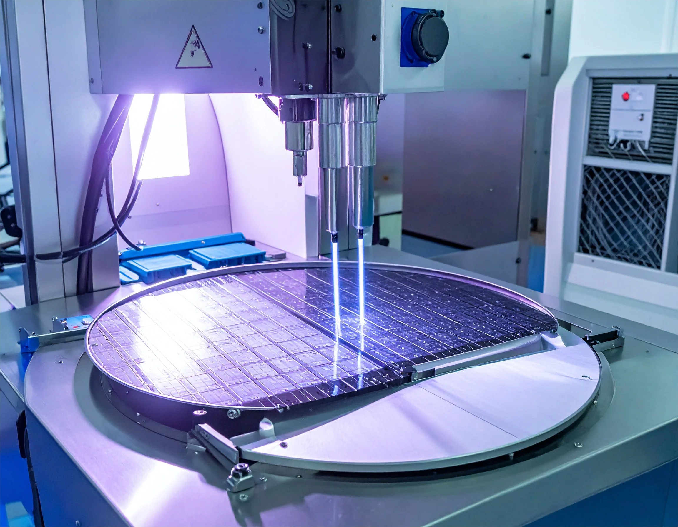
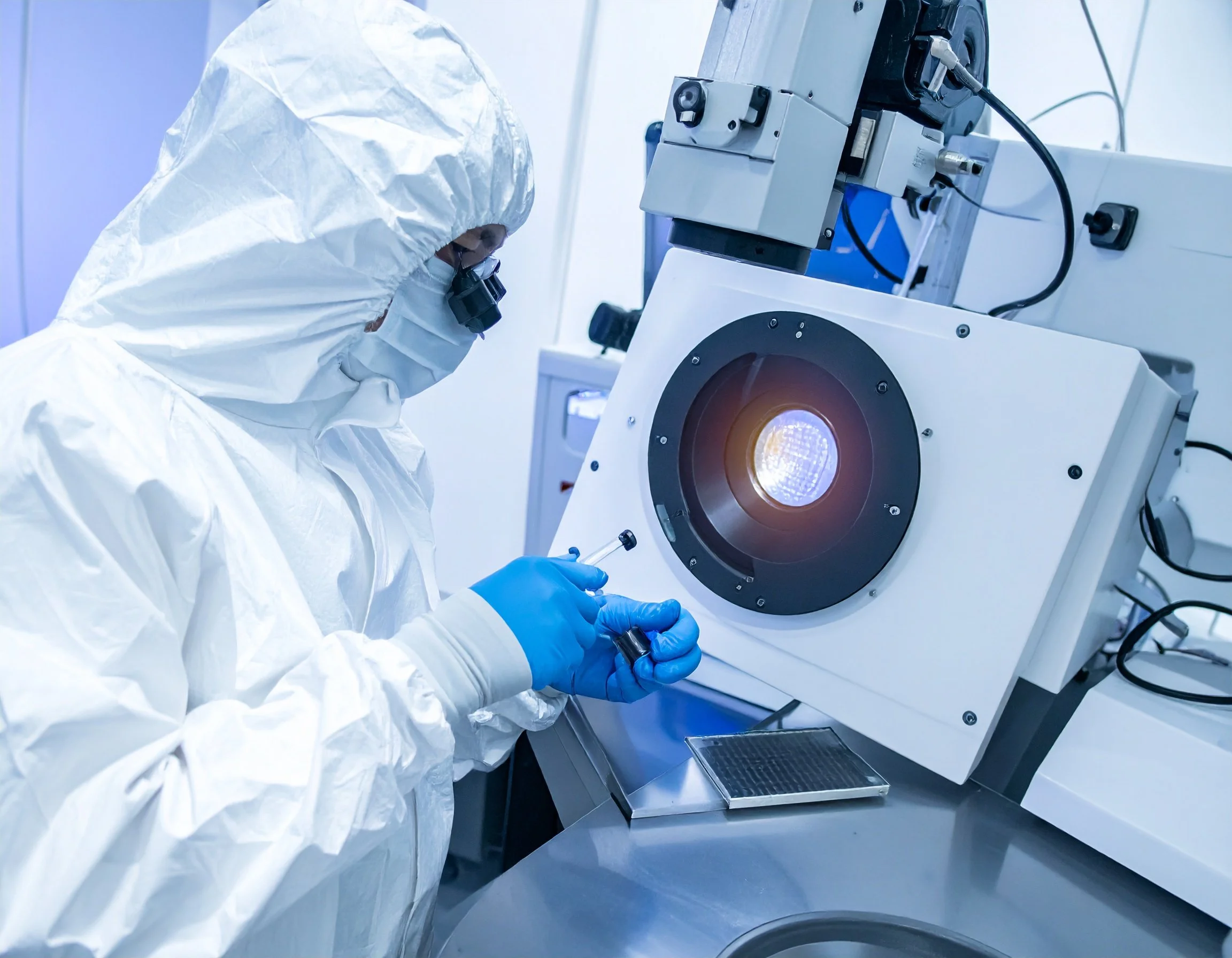
How atomic-level cleaning technologies help meet challenges in medical ICs
In medical integrated circuits (ICs), ensuring the highest quality and performance is critical. Medical ICs are used in a variety of sensitive applications, including diagnostic
Read More →

05/12/2025
Why Semiconductor R&D Teams Must Consider Atomic-Level Defects and Contamination in Chip Design
In the race to develop faster, smaller and more energy-efficient chips, design teams often focus intensely on architecture, functionality and scaling strategies. However, an often-underappreciated
Read More →
28/11/2025
Turning OSAT Challenges into Opportunities: How Sidewall Passivation Can Drive Yield and Market Advantage
Outsourced Semiconductor Assembly and Test (OSAT) providers operate in one of the most competitive segments of the semiconductor value chain. Margins are thin, customer expectations
Read More →
07/11/2025
AI at the Edge: Why Power Consumption Becomes Mission Critical
Edge devices — from smartphones to IoT sensors, wearables and remote embedded systems — are increasingly expected to run AI inference locally. The benefits are
Read More →
24/10/2025
How Atomic-Level Surface Defects and Contamination Drive Up Water Consumption in Semiconductor Fabrication
Atomic-level defects and contamination in semiconductor surfaces affect on the water consumption in semiconductor fabrication. Impurities have a significant impact on manufactured chip performance and
Read More →
17/10/2025
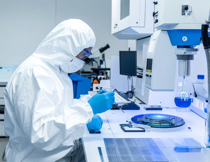
Atomic-Level Impurities in Semiconductor Interfaces: A Strategic Guide for Business Development Teams
In today’s advanced semiconductor manufacturing, reducing defect density defines the difference between average and world-class yield performance. SisuSemi’s atomic-level approach helps to eliminate microscopic impurities
Read More →

10/10/2025
Meeting the energy challenge: Smarter IoT, edge AI and mobile devices with SisuSemi
We are witnessing an unprecedented surge in connected devices. With nearly 20 billion IoT nodes already deployed—and close to 20 billion mobile devices in use—the
Read More →
03/10/2025
The Impact of Atomic-Level Impurities on Opto Components
In the world of semiconductors, the pursuit of perfection is a never-ending journey. Even the tiniest of imperfections, at the atomic level, can have a
Read More →

26/09/2025
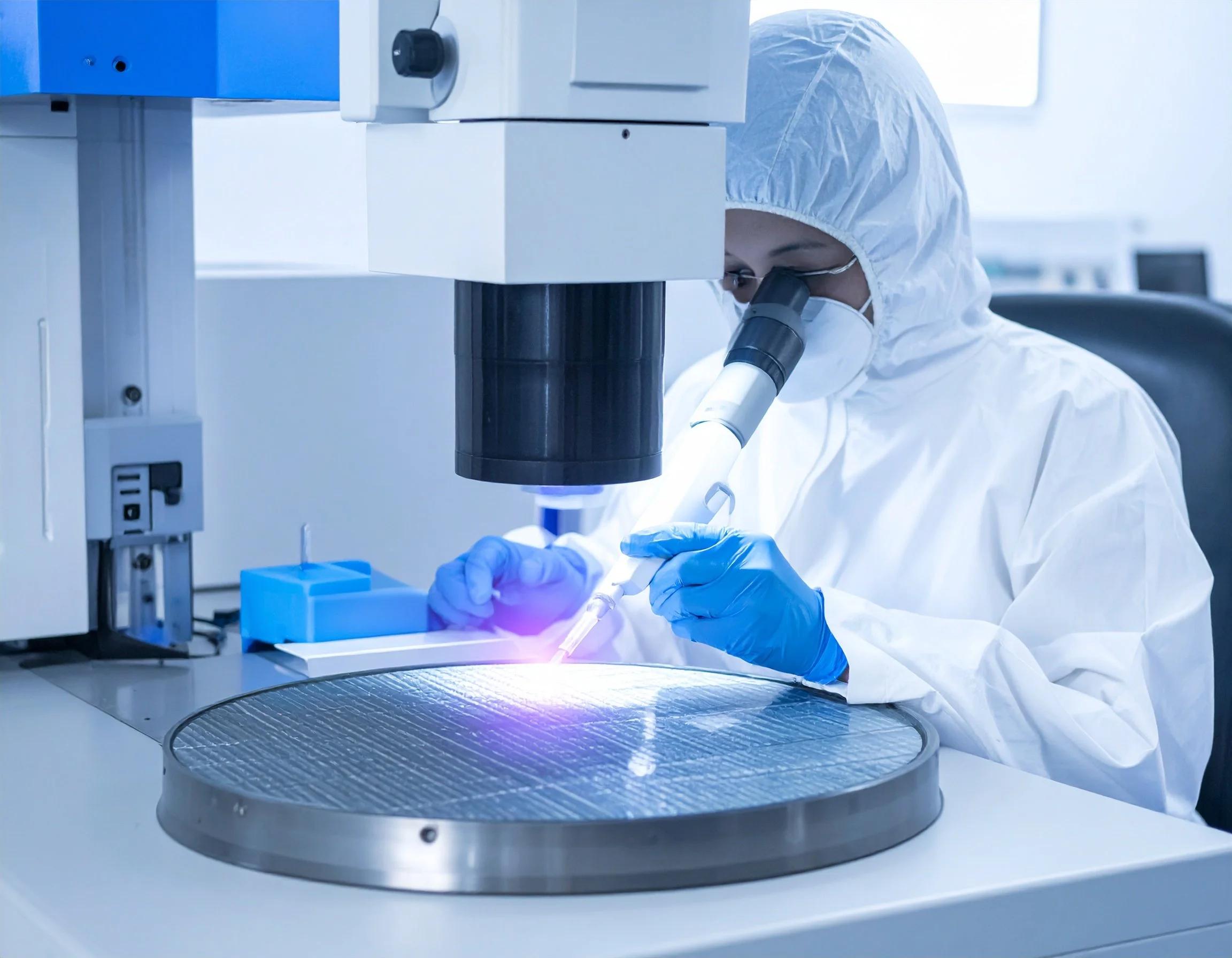
RCA Cleaning: Challenges at the Atomic Scale in Semiconductor Fabrication and How SisuSemi’s Ultra-High-Vacuum Technology Can Help
In semiconductor fabrication, cleanliness is extremely important — a single particle or impurity can cause major defects, impacting the performance and yield of the final
Read More →
19/09/2025
Atomic-Level Impurities: The Hidden Threat Undermining RF Semiconductor Performance—And How SisuSemi’s Technology is Changing the Game
In the age of 5G, IoT, satellite communication, radar and next-gen wireless infrastructure, radio frequency (RF) semiconductors are at the heart of our connected world.
Read More →